
Non-Reciprocal Quantum Wave Routing Device based on Wavefunction Collapse, Interference and Selective Absorption for integrated quantum and photonic systems
Quantentechnologien
Ref.-Nr.: 1201-5691-FG
Background
Non-reciprocal devices are indispensable in microwave engineering, photonics and quantum technologies, where they protect sensitive components from back reflections and enable directional signal routing. Conventional isolators and circulators generally rely on magneto-optical materials or complex active control schemes, which may limit miniaturization, integration and compatibility with emerging quantum technologies.
Technology
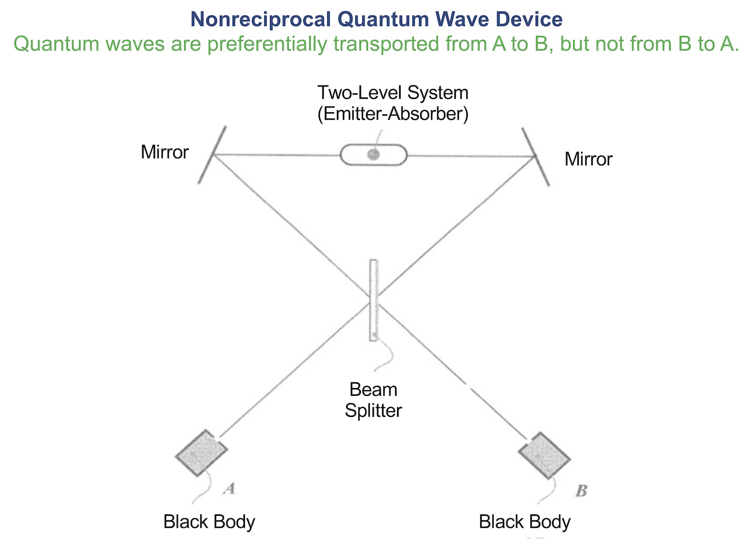
The invention relates to a quantum device comprising a transmission structure configured to achieve nonreciprocal transport of quantum waves through the combined action of quantum interference, wavefunction collapse and selective absorption. The inventive concept intends to preferentially direct quantum waves between two or more ports by controlling their propagation through specially designed transmission paths.
The invention relates to several embodiments, including:
- a photonic implementation employing an asymmetric half-transparent mirror, conventional mirrors and an absorbing/re-emitting quantum system;
- an electronic implementation based on asymmetric tunnel junctions and three-terminal junctions;
- implementations using photons, electrons, phonons and other quantum particles or quasiparticles.
The transmission structure generates multiple propagation paths that interfere depending on their phase relationship. Quantum-wave absorption and statistical re-emission introduce wavefunction collapse and phase randomization, resulting in preferential transport of quantum waves in one direction. The invention describes this mechanism as producing nonreciprocal motion of quantum waves between device ports.
Advantages
- Novel passive approach to achieving nonreciprocal quantum-wave transport.
- Applicable to multiple quantum carriers, including photons, electrons, phonons and quasiparticles.
- Compatible with integrated photonic and nanoelectronic platforms.
- Potential to reduce dependence on magneto-optic components or externally driven nonreciprocal devices.
- Flexible implementation using waveguides, optical components or electronic nanostructures.
Potential Applications
|
|
Patent Information
EP3850766A1, CN112753174B, JP7214844B2, JP7541796B2, US11569918B2
PDF Download
- Ref.-Nr.: 1201-5691-FG (221,6 KiB)
Kontaktperson

Patent- & Lizenzmanager
Dr. Franz Gadelmeier
Diplom-Physiker
+49 171 656 9140
gadelmeier@max-planck-innovation.de